Cameras have always dominated the electronics industry as it has lots of applications such as visitor monitoring system, surveillance system, attendance system etc. Cameras that we use today are smart and have a lot of features that were not present in earlier cameras. While todays digital cameras not only capture images but also captures high-level descriptions of the scene and analyse what they see. It is used extensively in Robotics, Artificial Intelligence, Machine Learning etc. The Captured frames are processed using Artificial Intelligence and Machine Learning, and then used in many applications like Number plate detection, object detection, motion detection, facial recognition etc.
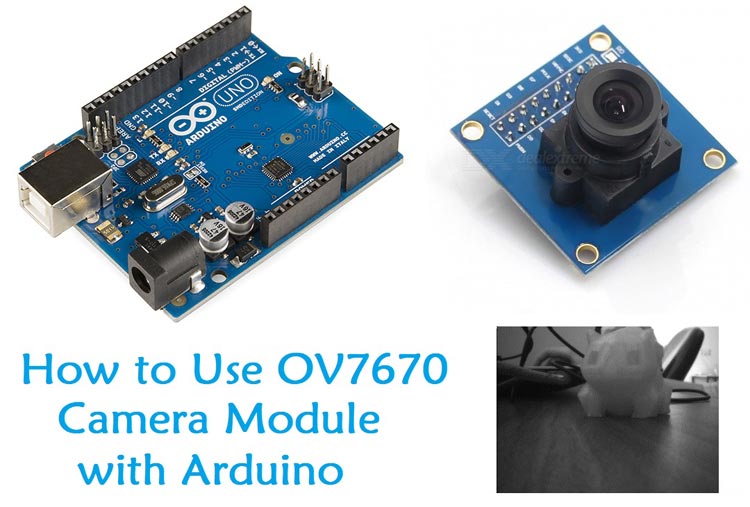
In this tutorial we will interface most widely used camera module OV7670 with Arduino UNO. The camera module OV7670 can be interfaced with Arduino Mega with same pin configuration, code and steps. The camera module is hard to interface because it has large number of pins and jumbled wiring to carry out. Also the wire becomes very important when using camera modules as the choice of the wire and length of the wire can significantly affect the picture quality and can bring noise.
We have already done ample projects on Cameras with different kind of Microcontrollers and IoT Devices such as:
- Visitor Monitoring System with Raspberry Pi and Pi Camera
- IOT based Raspberry Pi Home Security System with Email Alert
- Raspberry Pi Surveillance Camera with Motion Capture
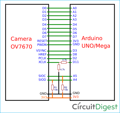
The Camera OV7670 works on 3.3V, so it becomes very important to avoid Arduino which gives 5V output at their Output GPIO pins. The OV7670 is a FIFO camera. But in this tutorial, the picture or frames will be grabbed without FIFO. This tutorial will have simple steps and simplified programming to interface OV7670 with Arduino UNO.
Components Required
- Arduino UNO
- OV7670 Camera Module
- Resistors(10k, 4.7k)
- Jumpers
Software Required:
- Arduino IDE
- Serial Port Reader (To analyze Output Image)
Things to Remember about Camera Module OV7670
OV7670 Camera Module is a FIFO camera Module available from different Manufacturers with different pin Configurations. TheOV7670 provides full frame, windowed 8-bit images in a wide range of formats. The image array is capable of operating at up to 30 frames per second (fps) in VGA. The OV7670 includes
- Image Sensor Array(of about 656 x 488 pixels)
- Timing Generator
- Analog Signal Processor
- A/D Converters
- Test Pattern Generator
- Digital Signal Processor(DSP)
- Image Scaler
- Digital Video Port
- LED and Strobe Flash Control Output
The OV7670 image sensor is controlled using Serial Camera Control Bus (SCCB) which is an I2C interface (SIOC, SIOD) with a maximum clock frequency of 400KHz.
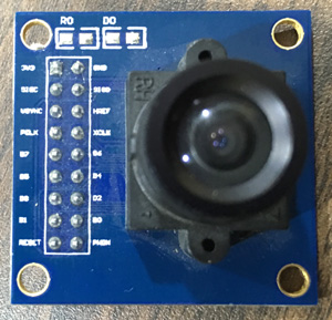
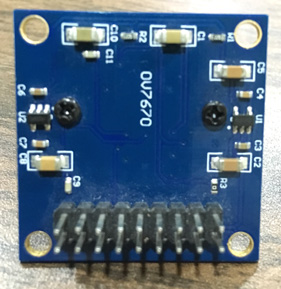
The Camera comes with handshaking signals such as:
- VSYNC: Vertical Sync Output – Low during frame
- HREF: Horizontal Reference – High during active pixels of row
- PCLK: Pixel Clock Output – Free running clock. Data is valid on rising edge
In addition to this, it has several more signals such as
- D0-D7: 8-bit YUV/RGB Video Component Digital Output
- PWDN: Power Down Mode Selection – Normal Mode and Power Down Mode
- XCLK: System Clock Input
- Reset: Reset Signal
The OV7670 is clocked from a 24MHz oscillator. This gives a Pixel Clock(PCLK) output of 24MHz. The FIFO provides 3Mbps of video frame buffer memory. The test pattern generator features 8-bar color bar pattern, fade-to-gray color bar patter. Now let’s start programming the Arduino UNO for testing Camera OV7670 and grabbing frames using serial port reader.
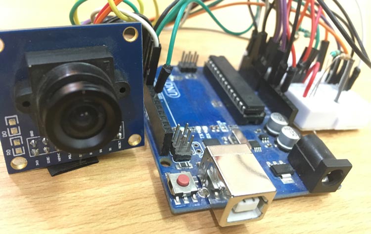
Circuit Diagram
Programming Arduino UNO
After this, the registers need to be modified for OV7670. The program is divided into small functions for better understanding.
The Setup() comprises all the initial setups required for only image capturing. The first function is arduinoUnoInut() which is used to initialise the arduino uno. Initially it disables all the global interrupts and sets the communication interface configurations such as the PWM clock, selection of interrupt pins, presclaer selection, adding parity and stop bits.
arduinoUnoInut();
After configuring the Arduino, the camera has to be configured. To initialise the camera, we only have the options to change the register values. The register values need to be changed from the default to the custom. Also add required delay depending upon the microcontroller frequency we are using. As, slow microcontrollers have less processing time adding more delay between capturing frames.
void camInit(void){
 writeReg(0x12, 0x80);
  _delay_ms(100);
  wrSensorRegs8_8(ov7670_default_regs);
 writeReg(REG_COM10, 32);//PCLK does not toggle on HBLANK.
}
The camera is set to take a QVGA image so the resolution need to be selected. The function configures the register to take a QVGA image.
setResolution();
In this tutorial, the images are taken in monochrome, so the register value is set to output a monochrome image. The function sets the register values from register list which is predefined in the program.
setColor();
The below function is write to register function which writes the hex value to register. If you get the scrambled images then try to change the second term i.e. 10 to 9/11/12. But most of the time this value works fine so no need to change it.
writeReg(0x11, 10);
This function is used to get the image resolution size. In this project we are taking pictures in the size of 320 x 240 pixels.
captureImg(320, 240);
Other than this, the code also has the I2C configurations divided in to several parts. Just to get the data from camera, the I2C configurations has Start, Read, Write, Set Address function which are important when using I2C protocol.
You can find the complete code with a demonstration video at the end of this tutorial. Just Upload the code and open the Serial Port Reader and grab the frames.
How to Use Serial Port Reader for reading Images
Step 1: Connect Your Arduino to any USB Port of your PC
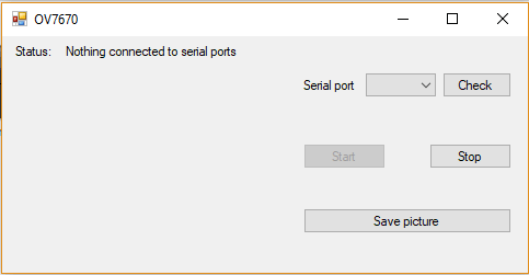
Step 2: Click on “Check” to find your Arduino COM Port
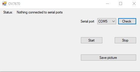
Step 3: Finally click on “Start” button to start reading serially.
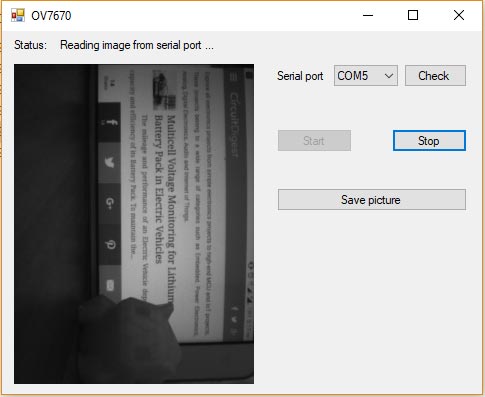
Step 4: One can also save this pictures by just clicking on “Save Picture”.
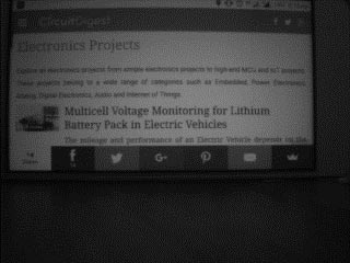
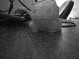
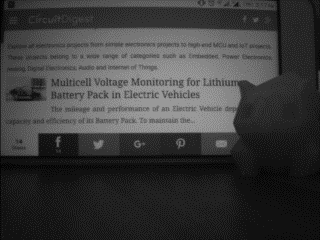
Below are Sample Images Taken from the OV7670
Precautions when using OV7670
- Try to use wires or jumpers as short as possible
- Avoid any loose contact to any pins on Arduino or OV7670
- Be careful about connecting as large number of wiring can lead short circuit
- If the UNO gives 5V output to GPIO then use Level Shifter.
- Use 3.3V Input for OV7670 as exceeding voltage than this can damage the OV7670 module.
This project is created to give overview of using a camera module with Arduino. Since Arduino has less memory, so the processing may not be as expected. You can use different controllers which has more memory for processing.
#include <stdint.h>
#include <avr/io.h>
#include <util/twi.h>
#include <util/delay.h>
#include <avr/pgmspace.h>
#define F_CPU 16000000UL
#define vga 0
#define qvga 1
#define qqvga 2
#define yuv422 0
#define rgb565 1
#define bayerRGB 2
#define camAddr_WR 0x42
#define camAddr_RD 0x43
/* Registers */
#define REG_GAIN 0x00 /* Gain lower 8 bits (rest in vref) */
#define REG_BLUE 0x01 /* blue gain */
#define REG_RED 0x02 /* red gain */
#define REG_VREF 0x03 /* Pieces of GAIN, VSTART, VSTOP */
#define REG_COM1 0x04 /* Control 1 */
#define COM1_CCIR656 0x40 /* CCIR656 enable */
#define REG_BAVE 0x05 /* U/B Average level */
#define REG_GbAVE 0x06 /* Y/Gb Average level */
#define REG_AECHH 0x07 /* AEC MS 5 bits */
#define REG_RAVE 0x08 /* V/R Average level */
#define REG_COM2 0x09 /* Control 2 */
#define COM2_SSLEEP 0x10 /* Soft sleep mode */
#define REG_PID 0x0a /* Product ID MSB */
#define REG_VER 0x0b /* Product ID LSB */
#define REG_COM3 0x0c /* Control 3 */
#define COM3_SWAP 0x40 /* Byte swap */
#define COM3_SCALEEN 0x08 /* Enable scaling */
#define COM3_DCWEN 0x04 /* Enable downsamp/crop/window */
#define REG_COM4 0x0d /* Control 4 */
#define REG_COM5 0x0e /* All "reserved" */
#define REG_COM6 0x0f /* Control 6 */
#define REG_AECH 0x10 /* More bits of AEC value */
#define REG_CLKRC 0x11 /* Clocl control */
#define CLK_EXT 0x40 /* Use external clock directly */
#define CLK_SCALE 0x3f /* Mask for internal clock scale */
#define REG_COM7 0x12 /* Control 7 */ //REG mean address.
#define COM7_RESET 0x80 /* Register reset */
#define COM7_FMT_MASK 0x38
#define COM7_FMT_VGA 0x00
#define COM7_FMT_CIF 0x20 /* CIF format */
#define COM7_FMT_QVGA 0x10 /* QVGA format */
#define COM7_FMT_QCIF 0x08 /* QCIF format */
#define COM7_RGB 0x04 /* bits 0 and 2 - RGB format */
#define COM7_YUV 0x00 /* YUV */
#define COM7_BAYER 0x01 /* Bayer format */
#define COM7_PBAYER 0x05 /* "Processed bayer" */
#define REG_COM8 0x13 /* Control 8 */
#define COM8_FASTAEC 0x80 /* Enable fast AGC/AEC */
#define COM8_AECSTEP 0x40 /* Unlimited AEC step size */
#define COM8_BFILT 0x20 /* Band filter enable */
#define COM8_AGC 0x04 /* Auto gain enable */
#define COM8_AWB 0x02 /* White balance enable */
#define COM8_AEC 0x01 /* Auto exposure enable */
#define REG_COM9 0x14 /* Control 9- gain ceiling */
#define REG_COM10 0x15 /* Control 10 */
#define COM10_HSYNC 0x40 /* HSYNC instead of HREF */
#define COM10_PCLK_HB 0x20 /* Suppress PCLK on horiz blank */
#define COM10_HREF_REV 0x08 /* Reverse HREF */
#define COM10_VS_LEAD 0x04 /* VSYNC on clock leading edge */
#define COM10_VS_NEG 0x02 /* VSYNC negative */
#define COM10_HS_NEG 0x01 /* HSYNC negative */
#define REG_HSTART 0x17 /* Horiz start high bits */
#define REG_HSTOP 0x18 /* Horiz stop high bits */
#define REG_VSTART 0x19 /* Vert start high bits */
#define REG_VSTOP 0x1a /* Vert stop high bits */
#define REG_PSHFT 0x1b /* Pixel delay after HREF */
#define REG_MIDH 0x1c /* Manuf. ID high */
#define REG_MIDL 0x1d /* Manuf. ID low */
#define REG_MVFP 0x1e /* Mirror / vflip */
#define MVFP_MIRROR 0x20 /* Mirror image */
#define MVFP_FLIP 0x10 /* Vertical flip */
#define REG_AEW 0x24 /* AGC upper limit */
#define REG_AEB 0x25 /* AGC lower limit */
#define REG_VPT 0x26 /* AGC/AEC fast mode op region */
#define REG_HSYST 0x30 /* HSYNC rising edge delay */
#define REG_HSYEN 0x31 /* HSYNC falling edge delay */
#define REG_HREF 0x32 /* HREF pieces */
#define REG_TSLB 0x3a /* lots of stuff */
#define TSLB_YLAST 0x04 /* UYVY or VYUY - see com13 */
#define REG_COM11 0x3b /* Control 11 */
#define COM11_NIGHT 0x80 /* NIght mode enable */
#define COM11_NMFR 0x60 /* Two bit NM frame rate */
#define COM11_HZAUTO 0x10 /* Auto detect 50/60 Hz */
#define COM11_50HZ 0x08 /* Manual 50Hz select */
#define COM11_EXP 0x02
#define REG_COM12 0x3c /* Control 12 */
#define COM12_HREF 0x80 /* HREF always */
#define REG_COM13 0x3d /* Control 13 */
#define COM13_GAMMA 0x80 /* Gamma enable */
#define COM13_UVSAT 0x40 /* UV saturation auto adjustment */
#define COM13_UVSWAP 0x01 /* V before U - w/TSLB */
#define REG_COM14 0x3e /* Control 14 */
#define COM14_DCWEN 0x10 /* DCW/PCLK-scale enable */
#define REG_EDGE 0x3f /* Edge enhancement factor */
#define REG_COM15 0x40 /* Control 15 */
#define COM15_R10F0 0x00 /* Data range 10 to F0 */
#define COM15_R01FE 0x80 /* 01 to FE */
#define COM15_R00FF 0xc0 /* 00 to FF */
#define COM15_RGB565 0x10 /* RGB565 output */
#define COM15_RGB555 0x30 /* RGB555 output */
#define REG_COM16 0x41 /* Control 16 */
#define COM16_AWBGAIN 0x08 /* AWB gain enable */
#define REG_COM17 0x42 /* Control 17 */
#define COM17_AECWIN 0xc0 /* AEC window - must match COM4 */
#define COM17_CBAR 0x08 /* DSP Color bar */
/*
* This matrix defines how the colors are generated, must be
* tweaked to adjust hue and saturation.
*
* Order: v-red, v-green, v-blue, u-red, u-green, u-blue
* They are nine-bit signed quantities, with the sign bit
* stored in0x58.Sign for v-red is bit 0, and up from there.
*/
#define REG_CMATRIX_BASE 0x4f
#define CMATRIX_LEN 6
#define REG_CMATRIX_SIGN 0x58
#define REG_BRIGHT 0x55 /* Brightness */
#define REG_CONTRAS 0x56 /* Contrast control */
#define REG_GFIX 0x69 /* Fix gain control */
#define REG_REG76 0x76 /* OV's name */
#define R76_BLKPCOR 0x80 /* Black pixel correction enable */
#define R76_WHTPCOR 0x40 /* White pixel correction enable */
#define REG_RGB444 0x8c /* RGB 444 control */
#define R444_ENABLE 0x02 /* Turn on RGB444, overrides 5x5 */
#define R444_RGBX 0x01 /* Empty nibble at end */
#define REG_HAECC1 0x9f /* Hist AEC/AGC control 1 */
#define REG_HAECC2 0xa0 /* Hist AEC/AGC control 2 */
#define REG_BD50MAX 0xa5 /* 50hz banding step limit */
#define REG_HAECC3 0xa6 /* Hist AEC/AGC control 3 */
#define REG_HAECC4 0xa7 /* Hist AEC/AGC control 4 */
#define REG_HAECC5 0xa8 /* Hist AEC/AGC control 5 */
#define REG_HAECC6 0xa9 /* Hist AEC/AGC control 6 */
#define REG_HAECC7 0xaa /* Hist AEC/AGC control 7 */
#define REG_BD60MAX 0xab /* 60hz banding step limit */
#define REG_GAIN 0x00 /* Gain lower 8 bits (rest in vref) */
#define REG_BLUE 0x01 /* blue gain */
#define REG_RED 0x02 /* red gain */
#define REG_VREF 0x03 /* Pieces of GAIN, VSTART, VSTOP */
#define REG_COM1 0x04 /* Control 1 */
#define COM1_CCIR656 0x40 /* CCIR656 enable */
#define REG_BAVE 0x05 /* U/B Average level */
#define REG_GbAVE 0x06 /* Y/Gb Average level */
#define REG_AECHH 0x07 /* AEC MS 5 bits */
#define REG_RAVE 0x08 /* V/R Average level */
#define REG_COM2 0x09 /* Control 2 */
#define COM2_SSLEEP 0x10 /* Soft sleep mode */
#define REG_PID 0x0a /* Product ID MSB */
#define REG_VER 0x0b /* Product ID LSB */
#define REG_COM3 0x0c /* Control 3 */
#define COM3_SWAP 0x40 /* Byte swap */
#define COM3_SCALEEN 0x08 /* Enable scaling */
#define COM3_DCWEN 0x04 /* Enable downsamp/crop/window */
#define REG_COM4 0x0d /* Control 4 */
#define REG_COM5 0x0e /* All "reserved" */
#define REG_COM6 0x0f /* Control 6 */
#define REG_AECH 0x10 /* More bits of AEC value */
#define REG_CLKRC 0x11 /* Clocl control */
#define CLK_EXT 0x40 /* Use external clock directly */
#define CLK_SCALE 0x3f /* Mask for internal clock scale */
#define REG_COM7 0x12 /* Control 7 */
#define COM7_RESET 0x80 /* Register reset */
#define COM7_FMT_MASK 0x38
#define COM7_FMT_VGA 0x00
#define COM7_FMT_CIF 0x20 /* CIF format */
#define COM7_FMT_QVGA 0x10 /* QVGA format */
#define COM7_FMT_QCIF 0x08 /* QCIF format */
#define COM7_RGB 0x04 /* bits 0 and 2 - RGB format */
#define COM7_YUV 0x00 /* YUV */
#define COM7_BAYER 0x01 /* Bayer format */
#define COM7_PBAYER 0x05 /* "Processed bayer" */
#define REG_COM8 0x13 /* Control 8 */
#define COM8_FASTAEC 0x80 /* Enable fast AGC/AEC */
#define COM8_AECSTEP 0x40 /* Unlimited AEC step size */
#define COM8_BFILT 0x20 /* Band filter enable */
#define COM8_AGC 0x04 /* Auto gain enable */
#define COM8_AWB 0x02 /* White balance enable */
#define COM8_AEC 0x01 /* Auto exposure enable */
#define REG_COM9 0x14 /* Control 9- gain ceiling */
#define REG_COM10 0x15 /* Control 10 */
#define COM10_HSYNC 0x40 /* HSYNC instead of HREF */
#define COM10_PCLK_HB 0x20 /* Suppress PCLK on horiz blank */
#define COM10_HREF_REV 0x08 /* Reverse HREF */
#define COM10_VS_LEAD 0x04 /* VSYNC on clock leading edge */
#define COM10_VS_NEG 0x02 /* VSYNC negative */
#define COM10_HS_NEG 0x01 /* HSYNC negative */
#define REG_HSTART 0x17 /* Horiz start high bits */
#define REG_HSTOP 0x18 /* Horiz stop high bits */
#define REG_VSTART 0x19 /* Vert start high bits */
#define REG_VSTOP 0x1a /* Vert stop high bits */
#define REG_PSHFT 0x1b /* Pixel delay after HREF */
#define REG_MIDH 0x1c /* Manuf. ID high */
#define REG_MIDL 0x1d /* Manuf. ID low */
#define REG_MVFP 0x1e /* Mirror / vflip */
#define MVFP_MIRROR 0x20 /* Mirror image */
#define MVFP_FLIP 0x10 /* Vertical flip */
#define REG_AEW 0x24 /* AGC upper limit */
#define REG_AEB 0x25 /* AGC lower limit */
#define REG_VPT 0x26 /* AGC/AEC fast mode op region */
#define REG_HSYST 0x30 /* HSYNC rising edge delay */
#define REG_HSYEN 0x31 /* HSYNC falling edge delay */
#define REG_HREF 0x32 /* HREF pieces */
#define REG_TSLB 0x3a /* lots of stuff */
#define TSLB_YLAST 0x04 /* UYVY or VYUY - see com13 */
#define REG_COM11 0x3b /* Control 11 */
#define COM11_NIGHT 0x80 /* NIght mode enable */
#define COM11_NMFR 0x60 /* Two bit NM frame rate */
#define COM11_HZAUTO 0x10 /* Auto detect 50/60 Hz */
#define COM11_50HZ 0x08 /* Manual 50Hz select */
#define COM11_EXP 0x02
#define REG_COM12 0x3c /* Control 12 */
#define COM12_HREF 0x80 /* HREF always */
#define REG_COM13 0x3d /* Control 13 */
#define COM13_GAMMA 0x80 /* Gamma enable */
#define COM13_UVSAT 0x40 /* UV saturation auto adjustment */
#define COM13_UVSWAP 0x01 /* V before U - w/TSLB */
#define REG_COM14 0x3e /* Control 14 */
#define COM14_DCWEN 0x10 /* DCW/PCLK-scale enable */
#define REG_EDGE 0x3f /* Edge enhancement factor */
#define REG_COM15 0x40 /* Control 15 */
#define COM15_R10F0 0x00 /* Data range 10 to F0 */
#define COM15_R01FE 0x80 /* 01 to FE */
#define COM15_R00FF 0xc0 /* 00 to FF */
#define COM15_RGB565 0x10 /* RGB565 output */
#define COM15_RGB555 0x30 /* RGB555 output */
#define REG_COM16 0x41 /* Control 16 */
#define COM16_AWBGAIN 0x08 /* AWB gain enable */
#define REG_COM17 0x42 /* Control 17 */
#define COM17_AECWIN 0xc0 /* AEC window - must match COM4 */
#define COM17_CBAR 0x08 /* DSP Color bar */
#define CMATRIX_LEN 6
#define REG_BRIGHT 0x55 /* Brightness */
#define REG_REG76 0x76 /* OV's name */
#define R76_BLKPCOR 0x80 /* Black pixel correction enable */
#define R76_WHTPCOR 0x40 /* White pixel correction enable */
#define REG_RGB444 0x8c /* RGB 444 control */
#define R444_ENABLE 0x02 /* Turn on RGB444, overrides 5x5 */
#define R444_RGBX 0x01 /* Empty nibble at end */
#define REG_HAECC1 0x9f /* Hist AEC/AGC control 1 */
#define REG_HAECC2 0xa0 /* Hist AEC/AGC control 2 */
#define REG_BD50MAX 0xa5 /* 50hz banding step limit */
#define REG_HAECC3 0xa6 /* Hist AEC/AGC control 3 */
#define REG_HAECC4 0xa7 /* Hist AEC/AGC control 4 */
#define REG_HAECC5 0xa8 /* Hist AEC/AGC control 5 */
#define REG_HAECC6 0xa9 /* Hist AEC/AGC control 6 */
#define REG_HAECC7 0xaa /* Hist AEC/AGC control 7 */
#define REG_BD60MAX 0xab /* 60hz banding step limit */
#define MTX1 0x4f /* Matrix Coefficient 1 */
#define MTX2 0x50 /* Matrix Coefficient 2 */
#define MTX3 0x51 /* Matrix Coefficient 3 */
#define MTX4 0x52 /* Matrix Coefficient 4 */
#define MTX5 0x53 /* Matrix Coefficient 5 */
#define MTX6 0x54 /* Matrix Coefficient 6 */
#define REG_CONTRAS 0x56 /* Contrast control */
#define MTXS 0x58 /* Matrix Coefficient Sign */
#define AWBC7 0x59 /* AWB Control 7 */
#define AWBC8 0x5a /* AWB Control 8 */
#define AWBC9 0x5b /* AWB Control 9 */
#define AWBC10 0x5c /* AWB Control 10 */
#define AWBC11 0x5d /* AWB Control 11 */
#define AWBC12 0x5e /* AWB Control 12 */
#define REG_GFI 0x69 /* Fix gain control */
#define GGAIN 0x6a /* G Channel AWB Gain */
#define DBLV 0x6b
#define AWBCTR3 0x6c /* AWB Control 3 */
#define AWBCTR2 0x6d /* AWB Control 2 */
#define AWBCTR1 0x6e /* AWB Control 1 */
#define AWBCTR0 0x6f /* AWB Control 0 */
struct regval_list{
uint8_t reg_num;
uint16_t value;
};
const struct regval_list qvga_ov7670[] PROGMEM = {
{ REG_COM14, 0x19 },
{ 0x72, 0x11 },
{ 0x73, 0xf1 },
{ REG_HSTART, 0x16 },
{ REG_HSTOP, 0x04 },
{ REG_HREF, 0xa4 },
{ REG_VSTART, 0x02 },
{ REG_VSTOP, 0x7a },
{ REG_VREF, 0x0a },
{ 0xff, 0xff }, /* END MARKER */
};
const struct regval_list yuv422_ov7670[] PROGMEM = {
{ REG_COM7, 0x0 }, /* Selects YUV mode */
{ REG_RGB444, 0 }, /* No RGB444 please */
{ REG_COM1, 0 },
{ REG_COM15, COM15_R00FF },
{ REG_COM9, 0x6A }, /* 128x gain ceiling; 0x8 is reserved bit */
{ 0x4f, 0x80 }, /* "matrix coefficient 1" */
{ 0x50, 0x80 }, /* "matrix coefficient 2" */
{ 0x51, 0 }, /* vb */
{ 0x52, 0x22 }, /* "matrix coefficient 4" */
{ 0x53, 0x5e }, /* "matrix coefficient 5" */
{ 0x54, 0x80 }, /* "matrix coefficient 6" */
{ REG_COM13, COM13_UVSAT },
{ 0xff, 0xff }, /* END MARKER */
};
const struct regval_list ov7670_default_regs[] PROGMEM = {//from the linux driver
{ REG_COM7, COM7_RESET },
{ REG_TSLB, 0x04 }, /* OV */
{ REG_COM7, 0 }, /* VGA */
/*
* Set the hardware window. These values from OV don't entirely
* make sense - hstop is less than hstart. But they work...
*/
{ REG_HSTART, 0x13 }, { REG_HSTOP, 0x01 },
{ REG_HREF, 0xb6 }, { REG_VSTART, 0x02 },
{ REG_VSTOP, 0x7a }, { REG_VREF, 0x0a },
{ REG_COM3, 0 }, { REG_COM14, 0 },
/* Mystery scaling numbers */
{ 0x70, 0x3a }, { 0x71, 0x35 },
{ 0x72, 0x11 }, { 0x73, 0xf0 },
{ 0xa2,/* 0x02 changed to 1*/1 }, { REG_COM10, 0x0 },
/* Gamma curve values */
{ 0x7a, 0x20 }, { 0x7b, 0x10 },
{ 0x7c, 0x1e }, { 0x7d, 0x35 },
{ 0x7e, 0x5a }, { 0x7f, 0x69 },
{ 0x80, 0x76 }, { 0x81, 0x80 },
{ 0x82, 0x88 }, { 0x83, 0x8f },
{ 0x84, 0x96 }, { 0x85, 0xa3 },
{ 0x86, 0xaf }, { 0x87, 0xc4 },
{ 0x88, 0xd7 }, { 0x89, 0xe8 },
/* AGC and AEC parameters. Note we start by disabling those features,
then turn them only after tweaking the values. */
{ REG_COM8, COM8_FASTAEC | COM8_AECSTEP },
{ REG_GAIN, 0 }, { REG_AECH, 0 },
{ REG_COM4, 0x40 }, /* magic reserved bit */
{ REG_COM9, 0x18 }, /* 4x gain + magic rsvd bit */
{ REG_BD50MAX, 0x05 }, { REG_BD60MAX, 0x07 },
{ REG_AEW, 0x95 }, { REG_AEB, 0x33 },
{ REG_VPT, 0xe3 }, { REG_HAECC1, 0x78 },
{ REG_HAECC2, 0x68 }, { 0xa1, 0x03 }, /* magic */
{ REG_HAECC3, 0xd8 }, { REG_HAECC4, 0xd8 },
{ REG_HAECC5, 0xf0 }, { REG_HAECC6, 0x90 },
{ REG_HAECC7, 0x94 },
{ REG_COM8, COM8_FASTAEC | COM8_AECSTEP | COM8_AGC | COM8_AEC },
{ 0x30, 0 }, { 0x31, 0 },//disable some delays
/* Almost all of these are magic "reserved" values. */
{ REG_COM5, 0x61 }, { REG_COM6, 0x4b },
{ 0x16, 0x02 }, { REG_MVFP, 0x07 },
{ 0x21, 0x02 }, { 0x22, 0x91 },
{ 0x29, 0x07 }, { 0x33, 0x0b },
{ 0x35, 0x0b }, { 0x37, 0x1d },
{ 0x38, 0x71 }, { 0x39, 0x2a },
{ REG_COM12, 0x78 }, { 0x4d, 0x40 },
{ 0x4e, 0x20 }, { REG_GFIX, 0 },
/*{0x6b, 0x4a},*/{ 0x74, 0x10 },
{ 0x8d, 0x4f }, { 0x8e, 0 },
{ 0x8f, 0 }, { 0x90, 0 },
{ 0x91, 0 }, { 0x96, 0 },
{ 0x9a, 0 }, { 0xb0, 0x84 },
{ 0xb1, 0x0c }, { 0xb2, 0x0e },
{ 0xb3, 0x82 }, { 0xb8, 0x0a },
/* More reserved magic, some of which tweaks white balance */
{ 0x43, 0x0a }, { 0x44, 0xf0 },
{ 0x45, 0x34 }, { 0x46, 0x58 },
{ 0x47, 0x28 }, { 0x48, 0x3a },
{ 0x59, 0x88 }, { 0x5a, 0x88 },
{ 0x5b, 0x44 }, { 0x5c, 0x67 },
{ 0x5d, 0x49 }, { 0x5e, 0x0e },
{ 0x6c, 0x0a }, { 0x6d, 0x55 },
{ 0x6e, 0x11 }, { 0x6f, 0x9e }, /* it was 0x9F "9e for advance AWB" */
{ 0x6a, 0x40 }, { REG_BLUE, 0x40 },
{ REG_RED, 0x60 },
{ REG_COM8, COM8_FASTAEC | COM8_AECSTEP | COM8_AGC | COM8_AEC | COM8_AWB },
/* Matrix coefficients */
{ 0x4f, 0x80 }, { 0x50, 0x80 },
{ 0x51, 0 }, { 0x52, 0x22 },
{ 0x53, 0x5e }, { 0x54, 0x80 },
{ 0x58, 0x9e },
{ REG_COM16, COM16_AWBGAIN }, { REG_EDGE, 0 },
{ 0x75, 0x05 }, { REG_REG76, 0xe1 },
{ 0x4c, 0 }, { 0x77, 0x01 },
{ REG_COM13, /*0xc3*/0x48 }, { 0x4b, 0x09 },
{ 0xc9, 0x60 }, /*{REG_COM16, 0x38},*/
{ 0x56, 0x40 },
{ 0x34, 0x11 }, { REG_COM11, COM11_EXP | COM11_HZAUTO },
{ 0xa4, 0x82/*Was 0x88*/ }, { 0x96, 0 },
{ 0x97, 0x30 }, { 0x98, 0x20 },
{ 0x99, 0x30 }, { 0x9a, 0x84 },
{ 0x9b, 0x29 }, { 0x9c, 0x03 },
{ 0x9d, 0x4c }, { 0x9e, 0x3f },
{ 0x78, 0x04 },
/* Extra-weird stuff. Some sort of multiplexor register */
{ 0x79, 0x01 }, { 0xc8, 0xf0 },
{ 0x79, 0x0f }, { 0xc8, 0x00 },
{ 0x79, 0x10 }, { 0xc8, 0x7e },
{ 0x79, 0x0a }, { 0xc8, 0x80 },
{ 0x79, 0x0b }, { 0xc8, 0x01 },
{ 0x79, 0x0c }, { 0xc8, 0x0f },
{ 0x79, 0x0d }, { 0xc8, 0x20 },
{ 0x79, 0x09 }, { 0xc8, 0x80 },
{ 0x79, 0x02 }, { 0xc8, 0xc0 },
{ 0x79, 0x03 }, { 0xc8, 0x40 },
{ 0x79, 0x05 }, { 0xc8, 0x30 },
{ 0x79, 0x26 },
{ 0xff, 0xff }, /* END MARKER */
};
void error_led(void){
DDRB |= 32;//make sure led is output
while (1){//wait for reset
PORTB ^= 32;// toggle led
_delay_ms(100);
}
}
void twiStart(void){
TWCR = _BV(TWINT) | _BV(TWSTA) | _BV(TWEN);//send start
while (!(TWCR & (1 << TWINT)));//wait for start to be transmitted
if ((TWSR & 0xF8) != TW_START)
error_led();
}
void twiWriteByte(uint8_t DATA, uint8_t type){
TWDR = DATA;
TWCR = _BV(TWINT) | _BV(TWEN);
while (!(TWCR & (1 << TWINT))) {}
if ((TWSR & 0xF8) != type)
error_led();
}
void twiAddr(uint8_t addr, uint8_t typeTWI){
TWDR = addr;//send address
TWCR = _BV(TWINT) | _BV(TWEN); /* clear interrupt to start transmission */
while ((TWCR & _BV(TWINT)) == 0); /* wait for transmission */
if ((TWSR & 0xF8) != typeTWI)
error_led();
}
voidwriteReg(uint8_t reg, uint8_t dat){
//send start condition
twiStart();
twiAddr(camAddr_WR, TW_MT_SLA_ACK);
twiWriteByte(reg, TW_MT_DATA_ACK);
twiWriteByte(dat, TW_MT_DATA_ACK);
TWCR = (1 << TWINT) | (1 << TWEN) | (1 << TWSTO);//send stop
_delay_ms(1);
}
static uint8_t twiRd(uint8_t nack){
if (nack){
TWCR = _BV(TWINT) | _BV(TWEN);
while ((TWCR & _BV(TWINT)) == 0); /* wait for transmission */
if ((TWSR & 0xF8) != TW_MR_DATA_NACK)
error_led();
return TWDR;
}
else{
TWCR = _BV(TWINT) | _BV(TWEN) | _BV(TWEA);
while ((TWCR & _BV(TWINT)) == 0); /* wait for transmission */
if ((TWSR & 0xF8) != TW_MR_DATA_ACK)
error_led();
return TWDR;
}
}
uint8_t rdReg(uint8_t reg){
uint8_t dat;
twiStart();
twiAddr(camAddr_WR, TW_MT_SLA_ACK);
twiWriteByte(reg, TW_MT_DATA_ACK);
TWCR = (1 << TWINT) | (1 << TWEN) | (1 << TWSTO);//send stop
_delay_ms(1);
twiStart();
twiAddr(camAddr_RD, TW_MR_SLA_ACK);
dat = twiRd(1);
TWCR = (1 << TWINT) | (1 << TWEN) | (1 << TWSTO);//send stop
_delay_ms(1);
return dat;
}
void wrSensorRegs8_8(const struct regval_list reglist[]){
uint8_t reg_addr, reg_val;
const struct regval_list *next = reglist;
while ((reg_addr != 0xff) | (reg_val != 0xff)){
reg_addr = pgm_read_byte(&next->reg_num);
reg_val = pgm_read_byte(&next->value);
writeReg(reg_addr, reg_val);
next++;
}
}
void setColor(void){
wrSensorRegs8_8(yuv422_ov7670);
// wrSensorRegs8_8(qvga_ov7670);
}
void setResolution(void){
writeReg(REG_COM3, 4); // REG_COM3 enable scaling
wrSensorRegs8_8(qvga_ov7670);
}
void camInit(void){
writeReg(0x12, 0x80);
_delay_ms(100);
wrSensorRegs8_8(ov7670_default_regs);
writeReg(REG_COM10, 32);//PCLK does not toggle on HBLANK.
}
void arduinoUnoInut(void) {
cli();//disable interrupts
/* Setup the 8mhz PWM clock
* This will be on pin 11*/
DDRB |= (1 << 3);//pin 11
ASSR &= ~(_BV(EXCLK) | _BV(AS2));
TCCR2A = (1 << COM2A0) | (1 << WGM21) | (1 << WGM20);
TCCR2B = (1 << WGM22) | (1 << CS20);
OCR2A = 0;//(F_CPU)/(2*(X+1))
DDRC &= ~15;//low d0-d3 camera
DDRD &= ~252;//d7-d4 and interrupt pins
_delay_ms(3000);
//set up twi for 100khz
TWSR &= ~3;//disable prescaler for TWI
TWBR = 72;//set to 100khz
//enable serial
UBRR0H = 0;
UBRR0L = 1;//0 = 2M baud rate. 1 = 1M baud. 3 = 0.5M. 7 = 250k 207 is 9600 baud rate.
UCSR0A |= 2;//double speed aysnc
UCSR0B = (1 << RXEN0) | (1 << TXEN0);//Enable receiver and transmitter
UCSR0C = 6;//async 1 stop bit 8bit char no parity bits
}
void StringPgm(const char * str){
do{
while (!(UCSR0A & (1 << UDRE0)));//wait for byte to transmit
UDR0 = pgm_read_byte_near(str);
while (!(UCSR0A & (1 << UDRE0)));//wait for byte to transmit
} while (pgm_read_byte_near(++str));
}
static void captureImg(uint16_t wg, uint16_t hg){
uint16_t y, x;
StringPgm(PSTR("*RDY*"));
while (!(PIND & 8));//wait for high
while ((PIND & 8));//wait for low
y = hg;
while (y--){
x = wg;
//while (!(PIND & 256));//wait for high
while (x--){
while ((PIND & 4));//wait for low
UDR0 = (PINC & 15) | (PIND & 240);
while (!(UCSR0A & (1 << UDRE0)));//wait for byte to transmit
while (!(PIND & 4));//wait for high
while ((PIND & 4));//wait for low
while (!(PIND & 4));//wait for high
}
// while ((PIND & 256));//wait for low
}
_delay_ms(100);
}
void setup(){
arduinoUnoInut();
camInit();
setResolution();
setColor();
writeReg(0x11, 10); //Earlier it had the value:writeReg(0x11, 12); New version works better for me :) !!!!
}
void loop(){
captureImg(320, 240);
}
Comments
it is given as a link in the
it is given as a link in the article itslef
Arduino Erros
it give me errors when compiling the code
any idea please ?
code download
can anyone send me a link of the code because im getting errors when compiling it
Arduino Yun is very different
Arduino Yun is very different from UNO, the MCU used on both boards are different. the code here will not work for Yun, atleast not wihout major madifications. so its better to get yourself a UNO
Hello,
Hello,
For some reason I keep getting very distored images, see below
I changed the value of 13 in this line "writeReg(0x11, 13);" to 9,10,11,12 and still got the same result.
I also played around with the camera lens by screwing/unscrewing it and I would still get this distored images.
Any other troubleshooting ideas?
Thank you in advance
I posted a more detailed
I posted a more detailed comment about what worked for me, but for some reason it is still "pending for approval". Let me summarize below:
- On line #535, change to OCR2A = 2; This set's the XCLK frequency to about 2.67MHz (instead of 8MHz).
- On line #590, change to writeReg(0x11, 31); This uses the CLKRC register to set the PCLK prescaler to 32 ie. PCLK frequency becomes 32 times slower than XCLK.
By making the above changes, the camera processing becomes slow enough for the Arduino Uno to be able to properly capture the images. In my case it took about 18.5s to capture an image.
OV7670 with Arduino Uno
Hello, thanks for the tutorials. I started trying to configure my OV7670 module about 2 weeks ago and decided to follow your tutorial since it looked easiest among the ones I had found, especially because of the SerialPortReader software which is well automated and does not require running many (or any) Command Prompt commands.
After a bit of a struggle I have finally got my camera module to work consistently. Like many other people, I also couldn't get the OV7670 camera working directly with this code on my Arduino Uno.
NB: First of all, if you copied this code directly, you would realize after compiling that there is an error on line #456 (voidwriteReg...). You just need to add a space between 'void' and 'writeReg', then the code will compile with no errors.
After that, these are the changes I eventually had to make to get my images to show finally:
- Make OCR2A = 2 (instead of 0) on line #535. This causes the XCLK to become about 2.667MHz (instead of 8MHz for OCR2A = 0)
- On line #590 which says writeReg(0x11, 10), change the second argument to 31, so that it becomes writeReg(0x11, 31). This, according to the datasheet, sets the PCLK prescaler to 32 (that is, the PCLK becomes 32 times slower than the XCLK).
The aim of the above changes is to get the camera timing signals (PCLK, HREF, VSYNC) running slow enough so that the Arduino Uno can accurately capture them and process the signals. With this arrangement, I was able to capture clear images. It takes about 18.5s to capture each image with this speed.
Also note that closing the camera lens all the way will most likely cause you to have an out of focus image so try to unscrew it a little. You can do the fine tuning once you start getting proper image output.
Before figuring this out I had to experiment a lot. For example I used I2C scanner at one point and found out that I could not get the camera working when the XCLK frequency (controlled by OCR2A) went below 2.667MHz.
Much of my success is attributed to the hardwork of Jorge Aparicio in his detailed but well-written post here, and also to MatanBright on this Arduino Forum post where he showed why the code would not work directly on my Arduino Mega, so that I advised myself to transfer my connections to the Uno. MatanBright also shared his solution for interfacing with the Arduino Mega which I plan to look into.
In the meantime, I am working on optimizing the code so that it can work more reliably at faster frame rates. I hope this helps someone.
Cheers!
JKAdofo
Still not getting images
Hi Jeromy,
Thanks so much for the detailed post. I tried following your directions, and am still not seeing any images when using the GUI. Was that the problem you were having intitially, and would you have any more suggestions for debugging? Thanks!
Hi Clare, I decided to check
Hi Clare, I decided to check back on this page after a long time and just discovered your question addressed to me. Have you been able to solve your problem now? If not, you can send a screenshot showing the kind of images you are getting. That would help a lot with the debugging.
in the whole code where is
in the whole code where is the final base64 format of image saved.
Also I would be very happy to
Also I would be very happy to get the source code for the SerialPortReader software so I can analyze it and make a few changes, such as the baud rate or probably output image size.
Thanks!
Make sure COM4 is the correct
Make sure COM4 is the correct Arduino COM number then consider the following:
- If COM4 is already open by another application (such as Arduino's Serial Monitor), then the software cannot access it.
- If COM4 has not been properly closed before you try to open it again by clicking the "Start" button. You may need to close the SerialPortReader software and reopen since sometimes clicking the "Stop" button does not close the port until an image has been captured.
COM 4 is the correct COM number
1) I didn't have arduino's serial monitor opened
2) This is what happen everytime and i tried to wait before but it didn't work.
THANK YOU MY MATE
It actually works after i try to rebuild everything and reuploading the code, thank you very much.
How you rebuild everything?
How you rebuild everything? I do this but not use.
The question for the connect pin
Hello sir,
Are the pin 3.3V and GND being common used between ov7670 and Uno in the circiut? Or it need to put other power supply to use?
Thanks.
Works great.
Worked for me first time, thanks for posting!
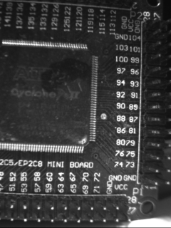
For everyone having problems compiling, find the line that has "voidwriteReg(uint8_t reg, uint8_t dat)" and put a space between the void and the function name i.e. "void writeReg(uint8_t reg, uint8_t dat)".
C:\Users\shuai\Desktop\sketch
C:\Users\shuai\Desktop\sketch_sep26ff\sketch_sep26ff.ino:7:0: warning: "F_CPU" redefined
#define F_CPU 16000000UL
^
How can i do this problem?
Hello, this tutorial works
Hello, this tutorial works fine for me but when I click on "Save Picture" and write a name for the photo, it says "Invalid name file". Someone can help please? Thanks
To save the picture, you need
To save the picture, you need to put the .bmp in the file name.
hello I donwloaded class
hello I donwloaded class stdint.h but dont work, of this site https://github.com/openbsd/src/blob/master/sys/sys/stdint.h
you can send me all classes???
#include <stdint.h>
#include <avr/io.h>
#include <util/twi.h>
#include <util/delay.h>
#include <avr/pgmspace.h>
thanks!"
The question for the connect pin
Hello sir,
I want to ask that 3.3V and GND pin are common or not?
Because the error that I made is identical with Aquoter and I already reset all thing but it still get error.
Thanks.
How to read video from camera
Has anybody know, how to do this tutorial on linux OS? Anybody know some software like Serial Port Reader for reading Images used here on Linux?
not capturing images
i uploaded same above code but image is not capturing and com port 3 is opened like tat showing tell me suggestions ....
Acessing Image Data Using Python
As the data is stored in a GUI. How to read the Image Matrix into a Python File ???
In the whole code where is
In the whole code where is the final base64 format of image saved
Serial Port Baud Rate
Hi All,
What is the Serial Port Baud Rate? I want to know what i should set the Arduino Serial Montor Baud Rate to?
Hi all,
Hi all,
Does anyone have an idea how to get the image uploaded directly online like to a web server etc.? I'll be very grateful. Just in case, my email is [email protected] i'm open to suggestions and discuttions.
Thanks
Hello!
Hello!
I was just poking around in the code, trying to make my own application to decode the data the camera sends over the serial port, but I could seem to figure out what encoding scheme is used in the code, so im not sure what to do with the data on the other side once ive received it.
Any help would be welcome!
Are you able to recieve data
Are you able to recieve data at another side ?
Dear Ma'am / Sir
Dear Ma'am / Sir
I am Vishal , trying to interface OV7607 Cam with ESP8266, 12E , NodeMcu, but finding it very difficult , therefore requesting you all to please guide me so that I can complete my project,
Thanking you all in advance.
BUENAS NOCHES RECIEN VIENDO
BUENAS NOCHES RECIEN VIENDO SU TUTORIA L Y COMENTARIO ESPERANDO DE ANTEMANO ME SALGA FUNCIONANDO CORRECTAMENTE LO VISTO AQUI .
ES PRIMERA VEZ QUE VOY HACER LO QUE E VISTO DE ESTE TUTORIAL HASTA AQUI MUCHAS GRACIAS.
Hello, I would also like to…
Hello, I would also like to have the image in RGB, have you found how since? Thank you in advance.
Hi Abhimanyu Pandit, the…
Hi Abhimanyu Pandit, the FIFO camera I have has 22 pins, have you seen or use that model? I cannot come up with the proper pinout for it. The pins on mine are like this, has anyone one been able to use something similar?
|
CAMERA |
|
|
GND |
3V3 |
|
SIOD |
SIOC |
|
HREF |
VSY |
|
D6 |
D7 |
|
D4 |
D5 |
|
D2 |
D3 |
|
D0 |
D1 |
|
PWDN |
RST |
|
RCK |
STR |
|
OE |
WR |
|
RRST |
WRST |
Hi Abhimanyu Pandit, Are the…
Hi Abhimanyu Pandit,
Are the Serial Port Reader codes available?
I'm finding it difficult to program one in Java.
Thanks.
I can't find any of these…
I can't find any of these libraries. What should I do?
Can you please help me with…
Can you please help me with this, i am 3 days trying to figure this out, but its doesn't work out for me... :(



hello.
Can you send me the link where to download the software for serial port reader for images
thank you