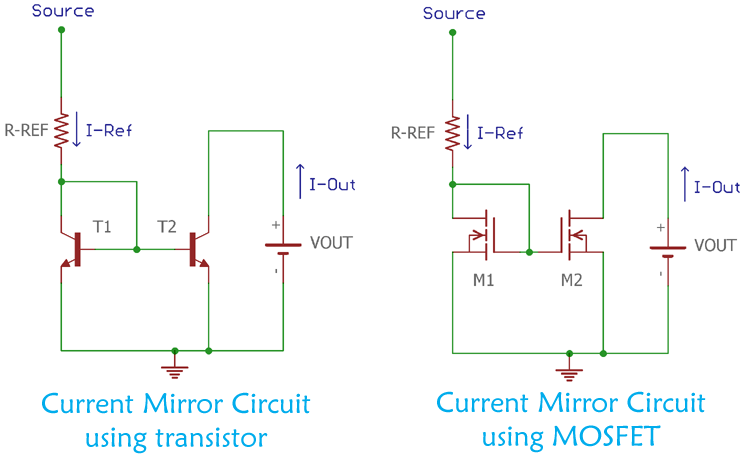
The Current Mirror is a widely popular technique for monolithic IC design. In this technique, the circuit is designed in such a way that it copies the current through one active device to another active device with current control feature. In this, the current is flowing through one device can be copied into another device but in inverting form. If the current of the first device is changed, the mirrored current output of the other device will also change. So by controlling the current in one device, the current in another device can also be controlled. Thus the current mirror circuit is often referred to a Current Controlled Current Source or CCCS.
Characteristic and Dependency of Current Mirror Circuit
A current mirror circuit has lots of primary and secondary dependencies and that is the main concern to characterize current mirror circuit.
A proper current mirror circuit can be characterized using three specifications.
1. Current Transfer Ratio
A current mirror circuit, mirror or copy the input current of one active device to the other active devices output. An ideal current mirror circuit is an ideal current amplifier with the inverting configuration that can reverse the current direction. Therefore, for an ideal current amplifier, the current transfer ratio is an important parameter.
2. AC output resistance
Resistance has a voltage-current relationship as per the ohms law. Thus, AC output resistance plays a major role in the stability of output current with respect to voltage changes.
3. Voltage drop
A proper working mirror circuit has a low voltage drop across the output. A voltage range in which a Current Mirror Circuit can work is called compliance range, and the minimum to maximum supported voltage in this compliances range is called as compliance voltage. A minimum voltage is required to keep the transistor in active mode, so the minimum voltage depends on the transistor specifications.
Limitations in Real Current Mirror Circuits
The ideal circuit and the real circuit, these two are completely different. In the real world, there is nothing called perfect or ideal. However, before understanding the limitations of current mirror circuits with respect of real-world applications, one needs to understand the voltage and current source and their ideal and actual behaviors.
A voltage source is a device which is capable to provide fixed and stable voltage to the load. In ideal terminology, the voltage source will provide a fixed voltage constantly without being dependent on the load current. Therefore, we can connect any load resistance across the ideal voltage source and get a stable and fixed voltage every time. This is not the case in real-world voltage source. In the real world, voltage sources like batteries, power supplies etc could not provide unlimited or infinite current to the loads.
Same as like the ideal voltage source, irrespective of the terminal voltage the current source can deliver or accept currents. But in the real world, the voltage also affects the constant current delivery process.
In the case of current mirror circuits, the voltage and current sources are ideal. But in a real scenario they have noises, tolerance, ripples thus the output voltage varies. This all affects the current mirror output.
Not only this, but theoretically in ideal current mirror circuits, the AC impedance is accepted as infinite, but this is not the case in real world scenario. The current mirror circuit in the practical world has finite impedance which affects the current delivery process. Also the circuit implementation creates parasitic capacitance which results in frequency limitation.
Current Mirror circuit using BJT
Bipolar junction transistors are widely used for current mirroring. The first trick to use bipolar junction transistor as a current mirror circuit is to construct an exponential voltage to current converter using the transistor. This is done by providing a voltage across the base-emitter junction of the BJT and the collector current is taken as an output. In this voltage to current converter configuration, simple negative feedback across the transistor converts the voltage to current converter properties to an opposite logarithmic current to voltage converter. Generally, the negative feedback is done by joining the base and the collector of the transistor.
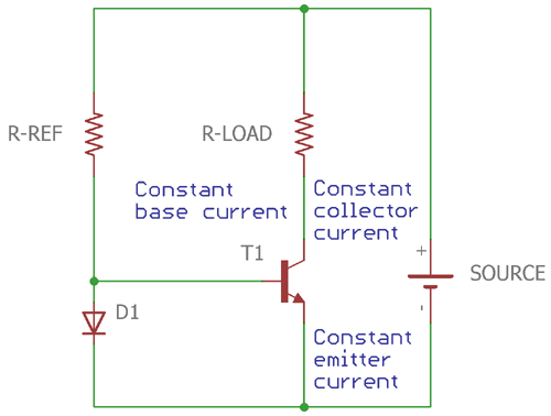
Let's consider the above image. Before understanding how the circuit works it is essential to understand the transistor operating characteristics. In the active mode operation, the transistor collector current can be calculated by multiplying the base current with the ratio of β. The ratio between emitter current and collector current is called ɑ. The relation between these two can be described using simple mathematical formation
ɑ = β/(β+1)
Therefore, a constant base-emitter voltage provides a constant emitter current. This constant emitter current which can be multiplied by constant ɑ ratio further provides a constant collector current.
In the previous image, a forward biased diode is used in parallel of the base-emitter junction which is providing constant voltage to the transistor. The voltage across the base-emitter is constant depending on the current flowing through the diode. However, the diode current can be controlled by the bias resistor. If the current through the diode is decreased by increasing the value of the bias resistance, the voltage drop across the diode will also reduce. By the effect of reduced base-emitter junction voltage, the emitter current will also decrease in the same proportion. One thing needs to be remembered that the ɑ and β of the transistor are constant.
By changing the diode current the emitter current of the transistor can be controlled. And by the same mean the collector current of the transistor can also be changed in the same proportion. By this rule, the emitter current of the transistor can be measured into the collector of the transistor. Thus, the bias resistor can control the collector current of the transistor.
This diode can be easily changed using a transistor which is same as the other counterpart.
In the below image, two transistors are shown which are used to create the current mirroring circuit. Transistor T1 and T2 need to be the same counterpart. Also, the two transistors should be placed close to each other for equal heat transfer.
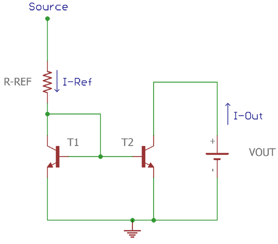
If we see the circuit carefully, the base-emitter of two transistors, T1 and T2 are in parallel with each other. Therefore, the two transistors have the same current. So, the best way to determine the output current is to add up the node current, where the IREF is flowing.
As per the Kirchhoff's law, the current at the T1 collector is –
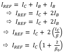
IREF = IC + IB1 + IB2
Therefore, when both transistors work with zero base-collector bias, the base currents are equal,
Base current of T1 (IB1) = Base current of T2 (IB2) = Total Base current of the node (IB)
The finite output resistance of the output transistor can be calculated using the below formula-
ROUT = VA + VCE / IC As per the R =V / I
The compliance voltage, where the VDG = 0 and the current mirror behavior still works in the lowest output voltage, can be calculated like this:
VCV = VT ln ((IC / IS) +1)) Where VT represents thermal voltage and IS is the scale current.
Current Mirror Technique using MOSFET
Current mirror circuit can be easily implemented using two MOSFET transistors. The working of the MOSFET current mirror circuit is similar as described in the previous transistor section.
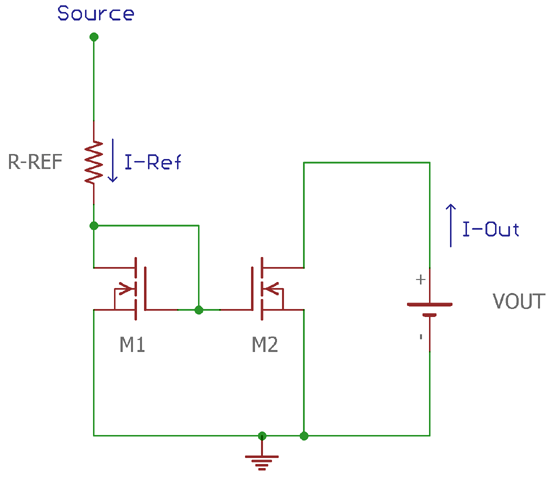
Consider the above current mirror circuit using MOSFET, the MOSFET transistor M1 is in the saturation region as the VDS ≤ VGS. For the case of MOSFET M2, it will also remain in saturation mode as long as the output voltage is greater than the saturation voltage. Therefore the input current across the M1 will control directly the output current of M2.
MOSFET device function like this, the drain current reflects the function of the gate to source and drain to gate voltage.
So, the formula can be written using the below function,
ID = f (VGS, VDG)
Due to this, the input current in the MOSFET M1, is mirrored to the drain current. In the image, the input current is provided by the bias resistor.
If the drain to gate voltage VDG is 0 for the MOSFET M1, the drain current of M1 will be
ID = f (VGS, VDG=0)
Therefore, f (VGS, 0) = IIN Thus, IIN sets the value of VGS.. The same gate to source voltage is reflected across the M2. So, if the M2 biased using zero
VDG and provided transistors M1 and M2 share identical properties and exact matching, then the
IOUT = f (VGS, VDG=0) is true.
So the output current is mirrored as the input current, IOUT = IIN
The drain-to-source voltage can be further introduced as VDS=VDG + VGS. With this changeover, the Shichman-Hodges model can provide the approximate answer of the f(VGS,VDG):
The function can be expressed as

Also, the output resistance can also be calculated as the output resistance is finite,

In the above formulas, KP is a transistor technology related constant, W/L is the ratio of Width and Length and λ is used for the modulation constant of channel length.
VGS, Vth and VDS are gate to source voltage, threshold voltage and drain to source voltage respectively.
The compliance voltage, where the VDG = 0 and the output MOSFET resistance is still high, current mirror behaviour still works in the lowest output voltage. The compliance voltage can be calculated by deriving the condition –
VCV = VGS (ID at VDG = 0)
Or, f-1 (ID) when the VDG = 0
Practical Model for Current Mirror Circuit
The current mirror circuit is simulated using Proteus models.
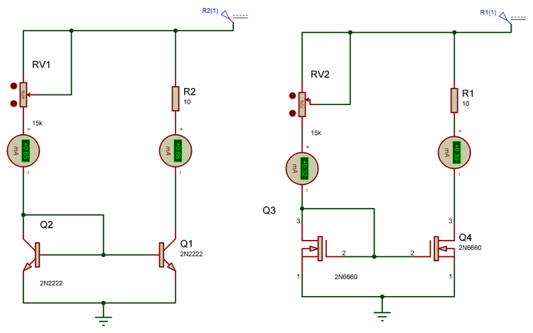
In the left side, the current mirror circuit using 2N2222 BJT is shown where two identical transistor pair is used. Instead of the programming resistor, a potentiometer is used to control the current flow in the live simulation. This same thing is created for the 2N6660 MOSFETs.
An amp meter is connected on both input and output current side. As the simulation goes, the input current is almost same and reflecting across the secondary side.
The in detail working can be seen in the Video given below.
Applications of Current Mirror Circuit
There are wide applications of Current Mirror Circuit in the field of integrated circuit manufacturing. The reference current source is created using the current mirror circuit. By using this technique, multiple reference points can be created from a single source. Hence, changing one reference point also change the current source across different parts of the circuit.


